ASML is on track to ship the industry's first extreme ultraviolet (EUV) lithography scanner with a 0.55 numerical aperture (NA) this year, the company's chief executive said this week. ASML's Twinscan EXE:5000 machine will be primarily used for development purposes and getting the company's customers familiar with the new technology as well as its capabilities. Commercial usage of High-NA tools is slated for 2025 and beyond.
"A few suppliers had some difficulties in actually ramping up and also giving us the right level of technological quality, so that led to some delay," said Peter Wennink, chief executive of ASML, in a conversation with Reuters. "But in fact, the first shipment is still this year.
This year ASML will ship its Twinscan EXE:5000 scanner to one undisclosed customer. The client will likely be Intel as the company once publicly disclosed plans to use High-NA scanners for its 18A process technology — but eventually had to opt for a different solution involving EUV double patterning and pattern shaping using Applied Materials' Centura Sculpta system (as commercial Twinscan EXE:5200 scanners would only be available in 2025).

Intel will likely adopt ASML's High-NA tools for its post-18A process technologies, whereas its rivals from TSMC and Samsung will use them later in this decade. But those scanners are not going to be cheap. It is estimated that they may cost over $300 million per unit, which will further rise costs of leading-edge fabs.
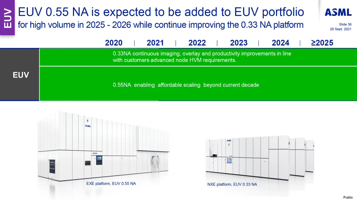
ASML's contemporary EUV scanners with a 0.33 NA and a 13nm resolution can print chips with metal pitches of around 30nm with single exposure patterning, which is good enough for production nodes like 5nm or 4nm-classes. For everything finer, chipmakers either need to use EUV double patterning or pattern shaping techniques, which is what they are going to be doing for the next couple of years. But beyond that they plan to use ASML's next-generation High-NA EUV scanners with a 0.55 NA and a resolution of around 8nm.
It is necessary to note that 0.55 NA EUV tools will not supplant the current deep ultraviolet (DUV) and EUV equipment in contemporary fabs, just like introduction of 0.33 NA EUV did not phase out DUV lithography. ASML will keep advancing its DUV and 0.33 NA EUV scanners for the foreseeable future. Concurrently, High-NA EUV lithography will play a pivotal role in shrinking transistor dimensions and boosting their performance.